第一作者:韩久慧、李琦、李超
通讯作者:韩久慧、陈明伟、丁轶
通讯单位:天津理工大学、南方科技大学
DOI: https://advanced.onlinelibrary.wiley.com/doi/10.1002/adma.202521570
(后附招聘信息)
1. 全文速览
在实现碳中和与氢能经济的大背景下,碱性水电解被认为是最具工业基础和规模化潜力的绿氢制备技术。然而,在安培级电流密度下,电极材料往往面临机械稳定性不足、界面结合差以及难以规模化制造等关键瓶颈,大多数实验室高性能催化剂因材料形态或制备工艺局限,难以直接应用于实际电解槽。
为突破这一瓶颈,天津理工大学韩久慧、丁轶教授和南方科技大学陈明伟教授团队提出一种“气相表面合金化–脱合金(VPA-CD)“新策略,可将普通商业金属板材直接原位转化为块体支撑纳米多孔电极,实现材料设计、结构构筑与器件制造的一体化。该策略成功构建Mo单原子掺杂纳米多孔Ni电极及Ni(Fe)/Ni₃Fe异质结构电极,在碱性水电解中实现安培级电流密度和长期稳定运行,并进一步成功构建了流场-催化一体化电解器件。
该研究建立了从块体金属→纳米多孔电极→器件级电解槽的可规模化制造新范式,为高电流密度绿氢制备提供了重要材料与工程技术基础。
2. 背景介绍
氢能被认为是未来可再生能源体系的重要组成部分,其中碱性水电解因技术成熟、成本低和工业基础完善而被广泛应用。然而,在实现大规模应用所需的安培级电流密度条件下,电极材料面临多方面挑战:
一方面,传统电催化剂多以粉体或薄膜形式存在,需通过粘结剂涂覆在金属基底上,界面结合力弱、电阻大,在高电流密度下易发生脱落与结构失效;另一方面,先进催化材料往往依赖复杂纳米结构设计,制备路线难以兼容工业规模制造,制约其工程应用。
近年来,尽管单原子催化剂、异质结构以及多孔电极等新型材料不断涌现,但如何实现高性能、机械稳定与规模化制造的统一仍是碱性水电解电极发展的核心科学与工程难题。因此,迫切需要发展一种能够直接从工业金属材料出发构筑高性能电极的新型制造策略。
3. 本文亮点
本工作提出一种可规模化气相表面合金化–脱合金(VPA-CD)策略,实现从商业金属板材到纳米多孔电极的直接转化,主要创新包括:
1)提出块体金属原位纳米多孔化制造新路线
通过气相Zn合金化与选择性脱合金过程,在块体金属表面原位构建纳米多孔催化层,并与基体形成冶金结合,实现高稳定一体化电极结构。
2)构建单原子与异质结构纳米多孔电极体系
成功制备Mo单原子掺杂纳米多孔Ni电极以及Ni(Fe)/Ni₃Fe异质结构电极,实现高效析氢与析氧协同催化。
3)实现安培级碱性水电解性能
构建的纳米多孔双电极体系在碱性电解中实现1.0 A cm⁻²电流密度,仅需1.84 V电压,并稳定运行185小时以上,性能优于商业电极。
4)提出流场-催化一体化电解器件新范式
利用气相合金化的高渗透能力,实现复杂流道结构表面均匀纳米多孔化,构建一体化电解槽结构,显著降低界面电阻并提升整体效率。
4. 图文解析
图1展示了VPA-CD策略的基本原理及结构演化过程。通过气相Zn合金化,在Ni基底表面形成均匀Ni-Zn表面合金层,随后通过选择性脱合金在表面生成纳米多孔Ni结构,并与致密基底形成冶金结合的一体化电极。该过程可在大面积金属板上均匀实现,并具备良好可重复性。
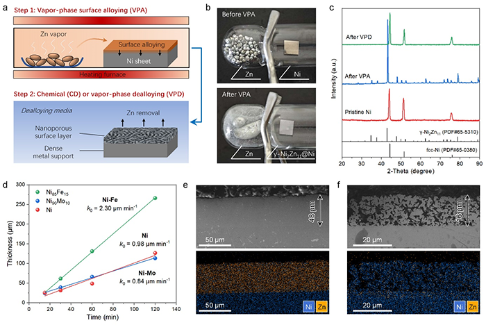
Figure 1 | Vapor-phase surface alloying–dealloying for in situ manufacturing of nanoporous Ni layers on bulk Ni sheets. (a) Schematic of the two-step process: Zn vapor-induced surface alloying (VPA) followed by selective dealloying—either chemical (CD) or vapor-phase dealloying (VPD)—to generate a nanoporous surface layer. (b) Experimental setup for VPA. (c) XRD patterns of Ni sheets in pristine, surface-alloyed (VPA 500 ℃, 1 h), and vapor-phase dealloyed states. (d) Thickness of the surface alloy layer as a function of VPA time at 500 ℃ for Ni, Ni90Mo10, and Ni85Fe15 sheets. (e) Cross-sectional SEM image and corresponding EDS mapping of the surface-alloyed Ni sheet (VPA 500 ℃, 1 h), showing a uniform γ-Ni2Zn11 layer. (f) Cross-sectional SEM image and EDS mapping of the vapor-phase dealloyed Ni sheet, showing a porous Ni surface layer metallurgically integrated with the dense Ni substrate.
图2系统展示Ni-Mo体系在VPA-CD过程中的结构演化。合金化后表面形成Zn富集层并伴随Mo析出相,脱合金后获得均匀纳米多孔Ni-Mo层。高分辨电镜表征表明,Mo不仅以纳米颗粒形式存在,还以单原子形式均匀分散于Ni纳米韧带中,形成Mo单原子掺杂纳米多孔Ni结构,为高效析氢提供活性位点。
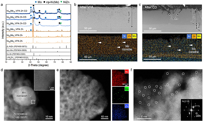
Figure 2 | Structural and morphological evolution of Ni–Mo alloys during the VPA-CD process. (a) XRD patterns of Ni98Mo2, Ni95Mo5, and Ni90Mo10 sheets in pristine, surface-alloyed (VPA 500 ℃, 2 h), and chemically dealloyed states. (b) Cross-sectional SEM image and EDS mapping of the surface-alloyed Ni90Mo10 sheet (VPA 500 ℃, 1 h), showing a uniform Zn-rich surface layer with embedded bcc-Mo precipitates. (c) Cross-sectional SEM image and EDS mapping of the chemically dealloyed Ni₉₀Mo₁₀ sheet, showing a conformal nanoporous Ni-Mo surface layer metallurgically bonded to the dense substrate with a thin β1-NiZn interlayer. (d) HAADF-STEM image of the nanoporous Ni–Mo layer, showing a Mo nanoparticle dispersed within the nanoporous Ni-Mo matrix. Inset: atomic-resolution lattice structure of the bcc-Mo nanoparticle. (e) HAADF-STEM image and EDS mapping of the nanoporous Ni-Mo matrix, showing Ni and residual Zn uniformly distributed, with weak Mo signals. (f) Atomic-resolution HAADF-STEM image of the nanoporous Ni-Mo matrix, revealing substitutional Mo single atoms (highlighted by white circles) dispersed within the Ni ligaments. Inset: corresponding fast Fourier transform (FFT) pattern.
图3展示Ni-Fe体系在VPA-CD过程中的结构演化。脱合金过程中形成纳米多孔Ni(Fe)骨架,并原位生成有序Ni₃Fe纳米颗粒,构建稳定异质界面结构,为高效析氧反应提供协同催化位点。
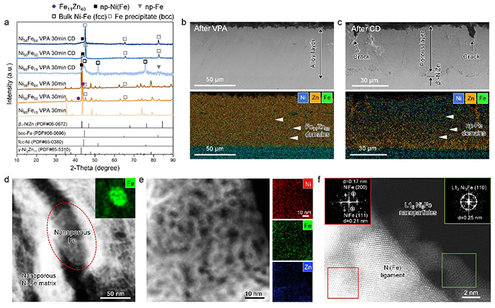
Figure 3 | Structural and morphological evolution of Ni–Fe alloys during the VPA-CD process. (a) XRD patterns of Ni85Fe15, Ni50Fe50, and Ni36Fe64 sheets in pristine, surface-alloyed (VPA 500 ℃, 30 min), and chemically dealloyed states. (b) Cross-sectional SEM image and EDS mapping of the surface-alloyed Ni85Fe15 sheet (VPA 500 ℃, 30 min), revealing a uniform Zn-rich surface layer with embedded Fe11Zn40 precipitates. (c) Cross-sectional SEM image and EDS mapping of the chemically dealloyed Ni₈₅Fe₁₅ sheet, showing a conformal nanoporous Ni–Fe surface layer metallurgically bonded to the dense substrate with a thin β1-NiZn interlayer. (d) HAADF-STEM image of the nanoporous Ni–Fe layer, showing a nanoporous Fe domain embedded within the nanoporous Ni-Fe matrix. Inset: EDS mapping highlighting Fe enrichment. (e) HAADF-STEM image and EDS mapping of the nanoporous Ni-Fe matrix, showing ~5 nm ligaments decorated with uniformly adhered 1–3 nm nanoparticles. (f) Atomic-resolution HAADF-STEM image of the nanoporous Ni-Fe matrix, revealing ordered L12-Ni3Fe nanoparticles adhered on fcc-Ni(Fe) ligaments. Inset: FFT patterns.
图4为电催化性能及稳定性测试结果。纳米多孔Ni–Mo电极在析氢反应中表现出优异活性,Ni(Fe)/Ni₃Fe电极在析氧反应中同样展现出卓越性能。基于该双电极体系构建的碱性电解装置在1.89 V即可实现1 A cm⁻²电流密度,并在100 mA cm⁻²电流密度下稳定运行120小时且无电压变化,显著优于商业对比电极。
对长期电解后的电极结构表征(图4j–l)表明,纳米多孔催化层与金属基底仍保持稳定结合,多孔骨架结构保持完整;纳米多孔Ni–Mo保持Mo单原子掺杂纳米多孔Ni结构,纳米多孔Ni–Fe发生表面重构,生成NiFeOOH活性相。
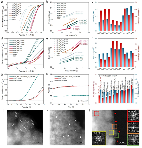
Figure 4 | Electrocatalytic performance and structural stability of bulk-metal-supported nanoporous electrodes for alkaline water splitting. (a) HER polarization curves of nanoporous Ni–Mo, Ni–Fe, and Ni electrodes with different alloy compositions, compared with commercial JAMC and JAFC cathodes. (b) Corresponding HER Tafel plots. (c) HER overpotentials at 200 mA cm–2geo (η200) and Tafel slopes, highlighting np-Ni90Mo10-2 h as the most active HER electrode. (d) OER polarization curves of nanoporous Ni–Mo, Ni–Fe, and Ni electrodes, compared with commercial JAMA and JAFA anodes. (e) Corresponding OER Tafel plots. (f) OER overpotentials at 200 mA cm–2geo (η200) and Tafel slopes, showing np-Ni85Fe15-30 min as the most active OER electrode. (g) Two-electrode overall water splitting performance using np-Ni90Mo10-2 h as the cathode and np-Ni85Fe15-30 min as the anode, compared with commercial electrode pairs. (h) Durability test of overall water splitting at 100 mA cm–2geo for 120 h. (i) Benchmarking of HER and OER activities of nanoporous Ni–Mo and Ni–Fe electrodes against state-of-the-art catalysts reported in the literature. (j) Atomic-resolution HAADF-STEM image of the np-Ni90Mo10-2 h electrode after 120 h durability testing, revealing substitutional Mo single atoms (white circles) uniformly dispersed within the Ni ligaments. (k) HAADF-STEM image of the np-Ni85Fe15-30 min electrode after 120 h durability testing, showing retained nanoscale heterostructures with more diffuse contrast arising from surface oxide formation; decorated nanoparticles are indicated by white arrows. (l) Atomic-resolution HAADF-STEM image of the np-Ni85Fe15-30 min electrode after 120 h durability testing, revealing low-contrast surface oxide layers (red arrows) adhered to the ligament surfaces. Insets show the corresponding FFT patterns indexed to NiO and FeOOH phases.
图5中,研究团队进一步将VPA-CD策略拓展至大面积及复杂流道结构,实现流场与催化层一体化电极。构建的集成电解器件在2.0 V下电流密度达到1470 mA cm⁻²,并在1 A cm⁻²电流密度下可稳定运行超过185小时,展现出优异的工程应用潜力。
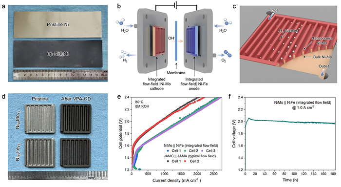
Figure 5 | Integrated “flow-field│catalyst” architectures enabled by VPA-CD. (a) Photograph of a large-area bulk-supported nanoporous Ni electrode (15 cm × 4.5 cm) fabricated via VPA-CD. (b) Schematic illustration of an alkaline water electrolyzer employing integrated “flow-field│catalyst” electrodes. (c) Schematic illustration of the structure of the integrated “flow-field│Ni-Mo” HER electrode. (d) Photograph of patterned Ni90Mo10 and Ni85Fe15 electrodes machined into serpentine flow-field structures before and after VPA-CD processing. (e) Polarization curves of the integrated electrolyzers using patterned nanoporous Ni90Mo10 cathodes paired with the nanoporous Ni85Fe15 anodes at 80 ℃ in 6 M KOH, compared with commercial JAMC/JAMA electrodes in a conventional electrolyzer with serpentine flow-field. (f) Long-term stability of the integrated electrolyzer operated at 1.0 A cm-2 for 185 h.
5.通讯作者介绍
韩久慧,天津理工大学教授,博士生导师,国家级青年人才项目入选者,国家重点研发计划(青年项目)首席科学家。2017年于日本东北大学获材料学博士学位,2017-2019和2020-2022年先后在日本东北大学材料科学高等研究所(AIMR)和学科交叉前沿科学研究所(FRIS)担任研究助手和助理教授,2022年入选国家级青年人才、天津理工大学“明理学者计划”领军人才。主要从事纳米多孔金属、电化学能源材料与器件、原位透射电子显微学研究。迄今在Adv. Mater., Nat. Comm., Nano Lett., Angew. Chem. Int. Ed., Adv. Energy Mater., Adv. Funct. Mater., Acta. Mater.等期刊发表SCI收录论文70余篇,被引6900余次。承担国家自然科学基金优青(海外)项目、国家重点研发计划“纳米前沿”青年科学家项目、国家重点研发计划“储能与智能电网技术”重点专项、日本学术振兴会(JSPS)项目等。曾获日本加藤科学振兴会研究奖、田中贵金属纪念财团MMS奖、日本东北大学“Prominent Research Fellow杰出研究员”等荣誉。担任eScience青年编委以及Science, Nat. Synth., Adv. Mater., Acta Mater.等国际学术期刊审稿人。详见个人网页:https://hanjiuhui.mysxl.cn/
课题组招聘(长期有效)
诚聘方向:原位透射电镜表征 | 电池材料 | 微纳电化学器件 | AI for Science
岗位:副教授(绿色通道,年薪30–40万元);师资博士后(年薪20–53万元)
联系方式:请发送简历至邮箱hanjh08@gmail.com
平台支撑:团队拥有完备的材料制备、表征、电化学测试、微纳器件检测设备。依托天津理工大学测试中心电子显微镜分中心,拥有7台先进的电镜设备(包括聚光镜球差校正透射电镜Titan Cubed Themis G2 300、物镜球差校正透射电镜Titan Themis Z、场发射透射电镜Talos F200X、透射电镜Tecnai G2 Spirit TWIN、聚焦离子束-电子束双束设备Helios NanoLab 460HP、场发射扫描电镜Verios 460L、场发射扫描电镜Quanta 250FEG),配备DPC、电子全息、4D-STEM和功能齐全的原位电、热、力、气、液样品杆。
欢迎海内外优秀青年学者加入团队,共同开展新能源材料与先进表征研究。