近日,武汉理工大学刘勇教授联合复旦大学赵东元院士团队,在光电子材料与器件领域取得新进展。研究团队提出B位低铅取代策略,通过调节激发态弛豫、电子结构并抑制深能级缺陷形成,在镉基二维Ruddlesden–Popper(RP)钙钛矿中实现了发光效率与双极性输运的协同提升,为兼顾高效发光与电荷输运的二维钙钛矿光电材料设计提供了新思路。相关成果以“Low Pb substitution unlocks Cd based Ruddlesden–Popper perovskites for bright emission and ambipolar transport”为题发表于国际纳米科学领域重要期刊ACS Nano上。武汉理工大学集成电路学院博士研究生唐子晟、材料学院博士研究生刘大民、硕士研究生庞哲为论文共同第一作者,武汉理工大学刘勇教授和复旦大学赵东元院士为论文通讯作者。
[研究背景]
二维RP卤化物钙钛矿凭借独特的层状量子阱结构和可调的光电特性,在发光器件与场效应晶体管等领域展现出重要应用潜力。然而,对于镉基二维RP钙钛矿,较强的激发态局域化影响其辐射复合路径,而深能级缺陷引起的非辐射复合与载流子俘获则严重制约其发光效率和电荷输运性能。因此,如何协同调控激发态弛豫并抑制深能级缺陷形成,实现发光与输运性能的协同提升,已成为该领域亟待突破的关键科学问题。
围绕这一问题,研究团队开发了一种B位低铅取代策略,通过Pb2+部分取代Cd2+构建了一系列的镉基二维RP相 (PA)2CsCd2−xPbxCl7 (x = 0−0.4) 钙钛矿,系统揭示了Pb2+取代比例对晶体结构、发光行为、电子结构及双极性输运的影响。其中,最优组分(x = 0.2)的光致发光量子产率(PLQY)由10.5%提高至80%,达到原来的约7.6倍;场效应晶体管的空穴和电子迁移率达到3.62和1.81 cm2 V−1 s−1,开关比最高达到8 × 10⁷,实现了发光与双极性输运性能的同步提升。
[研究内容]
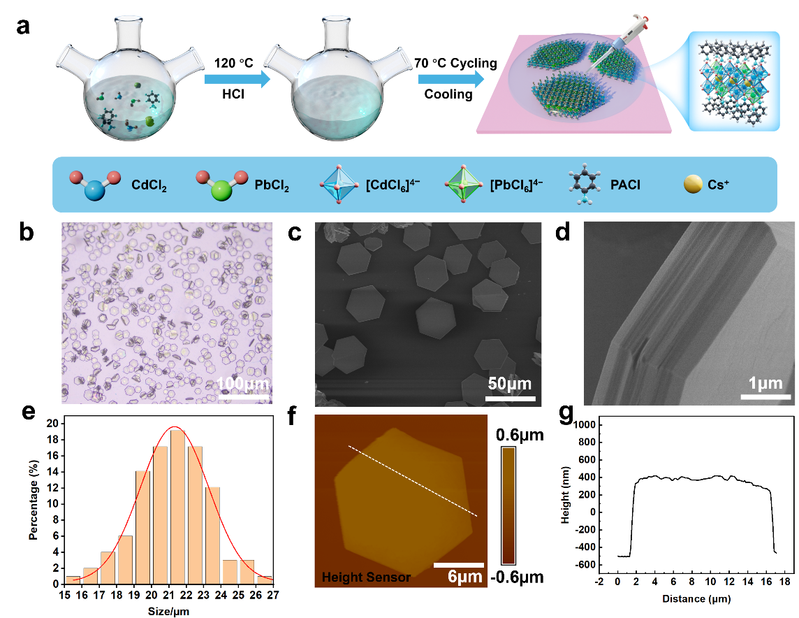
Figure 1. Synthesis and morphology characterization of 2D RP perovskite (PA)2CsCd1.8Pb0.2Cl7 microplates. (a) Schematic illustration of the synthesis strategy for (PA)2CsCd2−xPbxCl7. (b) OM image and (c) SEM image of (PA)2CsCd1.8Pb0.2Cl7. (d) Side-view image of (PA)2CsCd1.8Pb0.2Cl7. (e) Lateral-size distribution of (PA)2CsCd1.8Pb0.2Cl7. (f) AFM topography image of (PA)2CsCd1.8Pb0.2Cl7 and (g) corresponding height profile extracted along the white line in panel (f).
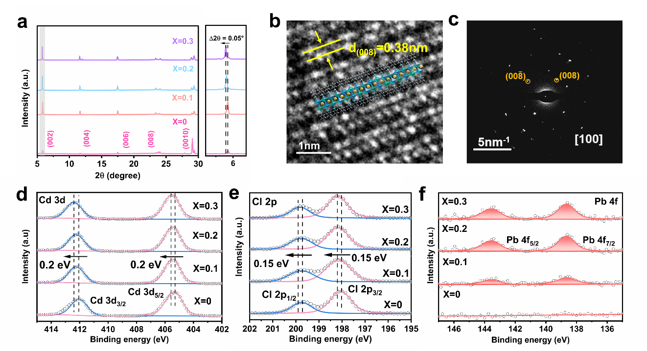
Figure 2. Structural and compositional characterization of (PA)2CsCd2-xPbxCl7 (x = 0, 0.1, 0.2, and 0.3). (a) XRD patterns of (PA)2CsCd2−xPbxCl7. Inset: Enlarged view of the selected diffraction region. (b) HRTEM image of (PA)2CsCd1.8Pb0.2Cl7 and (c) corresponding SAED pattern. XPS spectra of (d) Cd 3d, (e) Cl 2p, and (f) Pb 4f regions for (PA)2CsCd2−xPbxCl7.
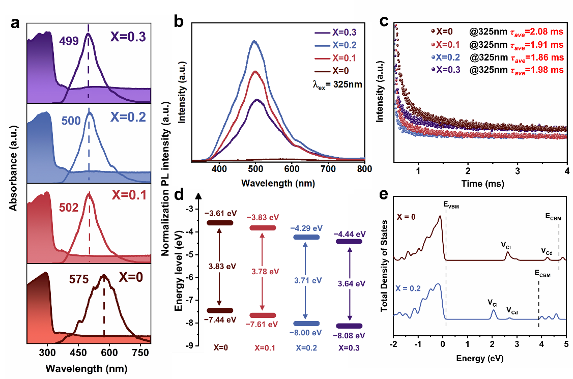
Figure 3. Optical properties and electronic structure of (PA)2CsCd2-xPbxCl7 (x = 0, 0.1, 0.2, and 0.3). (a) Normalized PL and UV–vis absorption spectra. (b) PL spectra. (c) TRPL decay curves. (d) Energy band structure. (e) Calculated TDOS of (PA)2CsCd2Cl7 and (PA)2CsCd1.8Pb0.2Cl7.
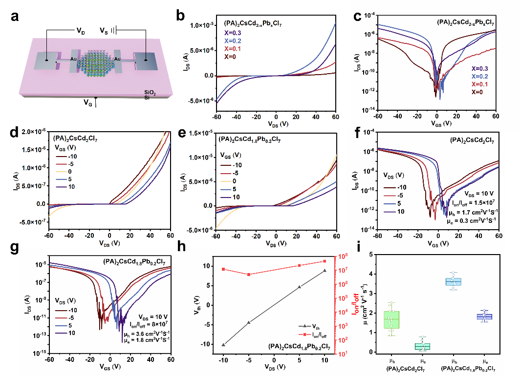
Figure 4. Field-effect transistor performance of (PA)2CsCd2-xPbxCl7 (x = 0, 0.1, 0.2, and 0.3). (a) Schematic illustration of the device structure. (b) Output and (c) transfer characteristics of (PA)2CsCd2−xPbxCl7. Output characteristics of (d) (PA)2CsCd2Cl7 and (e) (PA)2CsCd1.8Pb0.2Cl7 under different gate voltages. Transfer characteristics of (f) (PA)2CsCd2Cl7 and (g) (PA)2CsCd1.8Pb0.2Cl7 under different drain-source voltages. (h) Extracted Vth and Ion/Ioff of (PA)2CsCd1.8Pb0.2Cl7 as a function of drain-source voltage. (i) Statistical distributions of μh and μe obtained from 12 independent FET devices of (PA)2CsCd2Cl7 and (PA)2CsCd1.8Pb0.2Cl7.
[结论展望]
本研究采用B位低铅取代策略,协同调控激发态弛豫、缺陷形成与电子结构,实现了镉基二维RP钙钛矿发光效率与双极性输运性能的双重提升。研究表明,适量Pb2+的引入改变了(PA)2CsCd2Cl7骨架的局部化学环境与电子态分布,促进激发态复合向较高能量、较弱弛豫的辐射路径重新分配,同时提高缺陷形成能,从而有利于减少非辐射损耗和载流子俘获,实现了激发态行为与“缺陷—能带—输运”的协同调节。该研究不仅深化了对镉基二维RP钙钛矿组分、电子结构与光电性能之间关系的认识,也为兼顾高效发光与双极性输运的半导体材料设计及器件开发提供了新思路。
[论文信息]
Zisheng Tang, Zhe Pang, Damin Liu, Xiaoqian Wang, Jieheng Lv, Dafu Zhao, Manrui Liu, Chengqi Liu, Jiaqian Que, Kefeiyang Hu, Chong Peng, Xingbo Huang, Yingfei Liu, Dongyuan Zhao* and Yong Liu*; Low-Pb Substitution Unlocks Cd-Based Ruddlesden–Popper Perovskites for Bright Emission and Ambipolar Transport.
ACS Nano